- 您现在的位置:买卖IC网 > Sheet目录1902 > AT32UC3C2512C-A2UT (Atmel)IC MCU AVR32 512K FLASH 64TQFP
76
32117DS–AVR-01/12
AT32UC3C
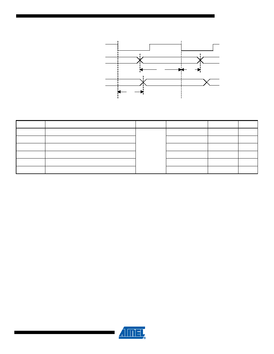
Figure 7-12. SPI Master Mode With (CPOL= 0 and NCPHA= 1) or (CPOL= 1 and NCPHA= 0)
Note:
1. These values are based on simulation and characterization of other AVR microcontrollers manufactured in the same pro-
cess technology. These values are not covered by test limits in production.
Maximum SPI Frequency, Master Output
The maximum SPI master output frequency is given by the following formula:
Where
is the MOSI delay, SPI2 or SPI5 depending on CPOL and NCPHA.
is the
maximum frequency of the SPI pins. Please refer to the I/O Pin Characteristics section for the
maximum frequency of the pins.
Maximum SPI Frequency, Master Input
The maximum SPI master input frequency is given by the following formula:
Where
is the MISO setup and hold time, SPI0 + SPI1 or SPI3 + SPI4 depending on
CPOL and NCPHA.
is the SPI slave response time. Please refer to the SPI slave
datasheet for
.
SPI3
SPI4
MISO
SPCK
MOSI
SPI5
Table 7-48.
SPI Timing, Master Mode(1)
Symbol
Parameter
Conditions
Min
Max
Units
SPI0
MISO setup time before SPCK rises
external
capacitor =
40pF
28.5+ (tCLK_SPI)/2
ns
SPI1
MISO hold time after SPCK rises
0
ns
SPI2
SPCK rising to MOSI delay
10.5
ns
SPI3
MISO setup time before SPCK falls
28.5 + (t
CLK_SPI)/2
ns
SPI4
MISO hold time after SPCK falls
0
ns
SPI5
SPCK falling to MOSI delay
10.5
ns
fSPCKMAX
MIN fPINMAX
1
SPIn
------------
(,
)
=
SPIn
fPINMAX
fSPCKMAX
1
SPIn tVALID
+
------------------------------------
=
SPIn
tVALID
发布紧急采购,3分钟左右您将得到回复。
相关PDF资料
AT32UC3C2512C-A2ZT
IC MCU 32BIT 512KB FLASH 64TQFP
AT32UC3L016-D3HR
MCU AVR32 16K FLASH 48TTLGA
AT42QT5480-CU QS444
IC SENSOR DUAL TOUCH 49-BGA
AT6010H-4QI
IC FPGA 4NS 240PQFP
AT80C31X2-SLRUM
MCU ROMLESS 31X2 5V 44-PLCC
AT80C51RD2-SLRUM
IC MCU 80C51 HI PERFORM 44PLCC
AT85C51SND3B1-RTTUL
IC DECODER/ENCODER DGTL 100-LQFP
AT87251G2D-RLTUM
IC MCU 8/16BIT 32K OTP 44-VQFP
相关代理商/技术参数
AT32UC3C2512C-A2ZR
功能描述:32位微控制器 - MCU 512KB FL,-40/125oC AUTO
RoHS:否 制造商:Texas Instruments 核心:C28x 处理器系列:TMS320F28x 数据总线宽度:32 bit 最大时钟频率:90 MHz 程序存储器大小:64 KB 数据 RAM 大小:26 KB 片上 ADC:Yes 工作电源电压:2.97 V to 3.63 V 工作温度范围:- 40 C to + 105 C 封装 / 箱体:LQFP-80 安装风格:SMD/SMT
AT32UC3C2512C-A2ZT
功能描述:32位微控制器 - MCU 512KB FL,-40/125oC AUTO
RoHS:否 制造商:Texas Instruments 核心:C28x 处理器系列:TMS320F28x 数据总线宽度:32 bit 最大时钟频率:90 MHz 程序存储器大小:64 KB 数据 RAM 大小:26 KB 片上 ADC:Yes 工作电源电压:2.97 V to 3.63 V 工作温度范围:- 40 C to + 105 C 封装 / 箱体:LQFP-80 安装风格:SMD/SMT
AT32UC3C2512C-Z2UR
制造商:Atmel Corporation 功能描述:MCU 32-bit AT32 AVR RISC 512KB Flash 3.3V/5V 64-Pin QFN EP T/R 制造商:Atmel Corporation 功能描述:512KB FLASH 64QFN(-40?C TO 85?C) T&R - Tape and Reel 制造商:Atmel Corporation 功能描述:IC MCU 32BIT 512KB FLASH 64QFN 制造商:Atmel Corporation 功能描述:32-bit Microcontrollers - MCU 512KB Flash 64QFN (-40oC to 85oC) 制造商:Atmel Corporation 功能描述:512KB Flash 64QFN(-40C to 85C) T&R
AT32UC3C2512C-Z2UT
制造商:Atmel Corporation 功能描述:512KFLASH AUTO - Trays
AT32UC3C2512C-Z2ZES
制造商:Atmel Corporation 功能描述:512KFLASH UC3C AUTO - QFN64 ENG SAMPLE - Bulk
AT32UC3C2512C-Z2ZR
功能描述:32位微控制器 - MCU 512KB FL,-40/125oC AUTO
RoHS:否 制造商:Texas Instruments 核心:C28x 处理器系列:TMS320F28x 数据总线宽度:32 bit 最大时钟频率:90 MHz 程序存储器大小:64 KB 数据 RAM 大小:26 KB 片上 ADC:Yes 工作电源电压:2.97 V to 3.63 V 工作温度范围:- 40 C to + 105 C 封装 / 箱体:LQFP-80 安装风格:SMD/SMT
AT32UC3C2512C-Z2ZT
功能描述:32位微控制器 - MCU 512KB FL,-40/125oC AUTO
RoHS:否 制造商:Texas Instruments 核心:C28x 处理器系列:TMS320F28x 数据总线宽度:32 bit 最大时钟频率:90 MHz 程序存储器大小:64 KB 数据 RAM 大小:26 KB 片上 ADC:Yes 工作电源电压:2.97 V to 3.63 V 工作温度范围:- 40 C to + 105 C 封装 / 箱体:LQFP-80 安装风格:SMD/SMT
AT32UC3C264C-A2UR
功能描述:32位微控制器 - MCU UC3C 64K FLASH 16K SRAM
RoHS:否 制造商:Texas Instruments 核心:C28x 处理器系列:TMS320F28x 数据总线宽度:32 bit 最大时钟频率:90 MHz 程序存储器大小:64 KB 数据 RAM 大小:26 KB 片上 ADC:Yes 工作电源电压:2.97 V to 3.63 V 工作温度范围:- 40 C to + 105 C 封装 / 箱体:LQFP-80 安装风格:SMD/SMT